
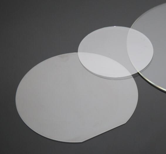
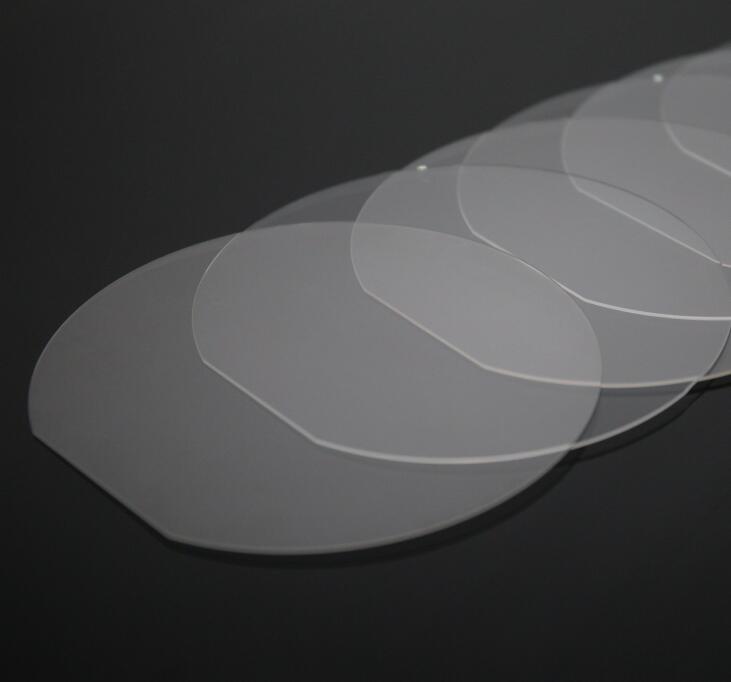
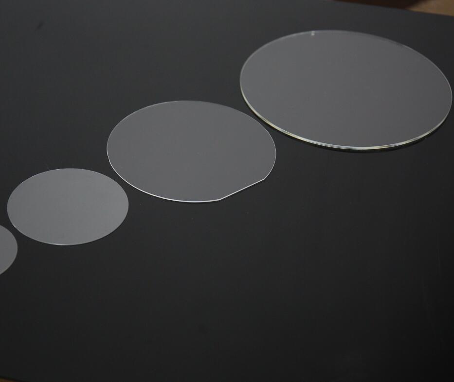
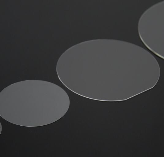


With many years of production experience, we can produce high-quality sapphire wafers of any crystal orientation, polished or unpolished. Through our polishing process, the thickness of sapphire wafers can be reduced, resulting in the desired thickness, as well as better TTV and lower surface roughness. Special crystal direction, with or without positioning edge can be customized according to customer requirements. For 1-inch C-side (0001) sapphire wafers, we usually offer round wafers without positioning edges.
|
Item |
1-inch C-plane(0001) 430μm Sapphire Wafers |
|
|
Crystal Materials |
99,999%, High Purity, Monocrystalline Al2O3 |
|
|
Grade |
Prime, Epi-Ready |
|
|
Surface Orientation |
C-plane(0001) C-plane off-angle toward M-axis 0.2 +/- 0.1° |
|
|
Diameter |
25.4 mm +/- 0.1 mm |
|
|
Thickness |
430 μm +/- 25 μm |
|
|
Single Side Polished |
Front Surface |
Epi-polished, Ra < 0.2 nm (by AFM) |
|
(SSP) |
Back Surface |
Fine ground, Ra = 0.8 μm to 1.2 μm |
|
Double Side Polished |
Front Surface |
Epi-polished, Ra < 0.2 nm (by AFM) |
|
(DSP) |
Back Surface |
Epi-polished, Ra < 0.2 nm (by AFM) |
|
TTV |
< 5 μm |
|
|
BOW |
< 5 μm |
|
|
WARP |
< 5 μm |
|
|
Cleaning / Packaging |
Class 100 cleanroom cleaning and vacuum packaging, 25 pieces in one cassette packaging or single piece packaging. |
|
|
Note: Sapphire wafer of any crystal direction and thickness can be customized according to customer requirements. |
||
2 inch Sapphire Wafers
We use a dedicated CMP (Chemical-Mechanical Polishing) technique to polish sapphire wafers, providing our customers with high surface quality sapphire wafers at a lower cost.
We have a wide range of standard sapphire wafers in stock to ensure fast delivery. Each chip is cleaned in a 100-level purification room with ultrapure water above 18 MΩ *cm and then packed in a clean cassette. 25 pieces/box or single piece box packaging to maximize research flexibility for customers.
|
Item |
2-inch C-plane(0001) 430μm Sapphire Wafers |
|
|
Crystal Materials |
99,999%, High Purity, Monocrystalline Al2O3 |
|
|
Grade |
Prime, Epi-Ready |
|
|
Surface Orientation |
C-plane(0001) C-plane off-angle toward M-axis 0.2 +/- 0.1° |
|
|
Diameter |
50.8 mm +/- 0.1 mm |
|
|
Thickness |
430 μm +/- 25 μm |
|
|
Primary Flat Orientation |
A-plane(11-20) +/- 0.2° |
|
|
Primary Flat Length |
16.0 mm +/- 1.0 mm |
|
|
Single Side Polished |
Front Surface |
Epi-polished, Ra < 0.2 nm (by AFM) |
|
(SSP) |
Back Surface |
Fine ground, Ra = 0.8 μm to 1.2 μm |
|
Double Side Polished |
Front Surface |
Epi-polished, Ra < 0.2 nm (by AFM) |
|
(DSP) |
Back Surface |
Epi-polished, Ra < 0.2 nm (by AFM) |
|
TTV |
< 10 μm |
|
|
BOW |
< 10 μm |
|
|
WARP |
< 10 μm |
|
|
|
Class 100 cleanroom cleaning and vacuum packaging,
25 pieces in one cassette packaging or single piece packaging. |
|
|
Note: Sapphire wafer of any crystal direction and thickness can be customized according to customer requirements. |
||
3 inch Sapphire Wafers
Sapphire chips are widely used in the growth and electronic applications of nitride epitaxial layers (GaN, AlN, InN, AlGaN, InGaN, InAlN, etc.). In these applications, the surface roughness of sapphire wafer is one of the key factors affecting its performance. We provide our customers with high surface quality sapphire wafers at low cost. For C-plane (0001) sapphire wafers, the roughness can be controlled to less than 0.2nm (AFM), and the roughness of special crystal directions (A-pane, R-plane, M-plane, N-plane, V-plane, etc.) can be controlled to less than 0.5nm (AFM).
|
Item |
3-inch C-plane(0001) 500μm Sapphire Wafers |
|
|
Crystal Materials |
99,999%, High Purity, Monocrystalline Al2O3 |
|
|
Grade |
Prime, Epi-Ready |
|
|
Surface Orientation |
C-plane(0001) C-plane off-angle toward M-axis 0.2 +/- 0.1° |
|
|
Diameter |
76.2 mm +/- 0.1 mm |
|
|
Thickness |
500 μm +/- 25 μm |
|
|
Primary Flat Orientation |
A-plane(11-20) +/- 0.2° |
|
|
Primary Flat Length |
22.0 mm +/- 1.0 mm |
|
|
Single Side Polished |
Front Surface |
Epi-polished, Ra < 0.2 nm (by AFM) |
|
(SSP) |
Back Surface |
Fine ground, Ra = 0.8 μm to 1.2 μm |
|
Double Side Polished |
Front Surface |
Epi-polished, Ra < 0.2 nm (by AFM) |
|
(DSP) |
Back Surface |
Epi-polished, Ra < 0.2 nm (by AFM) |
|
TTV |
< 15 μm |
|
|
BOW |
< 15 μm |
|
|
WARP |
< 15 μm |
|
|
Cleaning / Packaging |
Class 100 cleanroom cleaning and vacuum packaging, 25 pieces in one cassette packaging or single piece packaging. |
|
|
Note: Sapphire wafer of any crystal direction and thickness can be customized according to customer requirements. |
||
4 inch Sapphire Wafers
Sapphire wafers are widely used as substrates for III-V nitrides and many other epitaxial films. We offer 99.999% high purity sapphire wafers with excellent surface finish and smoothness to meet your high standards of use.
|
Item |
4-inch C-plane(0001) 650μm Sapphire Wafers |
|
|
Crystal Materials |
99,999%, High Purity, Monocrystalline Al2O3 |
|
|
Grade |
Prime, Epi-Ready |
|
|
Surface Orientation |
C-plane(0001) C-plane off-angle toward M-axis 0.2 +/- 0.1° |
|
|
Diameter |
100.0 mm +/- 0.1 mm |
|
|
Thickness |
650 μm +/- 25 μm |
|
|
Primary Flat Orientation |
A-plane(11-20) +/- 0.2° |
|
|
Primary Flat Length |
30.0 mm +/- 1.0 mm |
|
|
Single Side Polished |
Front Surface |
Epi-polished, Ra < 0.2 nm (by AFM) |
|
(SSP) |
Back Surface |
Fine ground, Ra = 0.8 μm to 1.2 μm |
|
Double Side Polished |
Front Surface |
Epi-polished, Ra < 0.2 nm (by AFM) |
|
(DSP) |
Back Surface |
Epi-polished, Ra < 0.2 nm (by AFM) |
|
TTV |
< 20 μm |
|
|
BOW |
< 20 μm |
|
|
WARP |
< 20 μm |
|
|
Cleaning / Packaging |
Class 100 cleanroom cleaning and vacuum packaging, 25 pieces in one cassette packaging or single piece packaging. |
|
|
Note: Sapphire wafer of any crystal direction and thickness can be customized according to customer requirements. |
||
5 inch Sapphire Wafers
5-inch C-side (0001) sapphire chips are not as common as other standard specifications. However, we use optically primary materials (99.999% high-purity Al2O3 single crystals) to produce high-quality 5-inch wafers with excellent surface finish and flatness, usually C-plane (0001) roughness less than 0.2 nm (via AFM). Or if you need customized sapphire wafers with special crystal orientation, thickness and size, please feel free to contact us. We will provide you with high surface quality sapphire wafers at a competitive cost.
|
Item |
5-inch C-plane(0001) 650μm Sapphire Wafers |
|
|
Crystal Materials |
99,999%, High Purity, Monocrystalline Al2O3 |
|
|
Grade |
Prime, Epi-Ready |
|
|
Surface Orientation |
C-plane(0001) C-plane off-angle toward M-axis 0.2 +/- 0.1° |
|
|
Diameter |
125.0 mm +/- 0.1 mm |
|
|
Thickness |
650 μm +/- 25 μm |
|
|
Primary Flat Orientation |
A-plane(11-20) +/- 0.2° |
|
|
Primary Flat Length |
42.0 mm +/- 1.0 mm |
|
|
Single Side Polished |
Front Surface |
Epi-polished, Ra < 0.2 nm (by AFM) |
|
(SSP) |
Back Surface |
Fine ground, Ra = 0.8 μm to 1.2 μm |
|
Double Side Polished |
Front Surface |
Epi-polished, Ra < 0.2 nm (by AFM) |
|
(DSP) |
Back Surface |
Epi-polished, Ra < 0.2 nm (by AFM) |
|
TTV |
< 20 μm |
|
|
BOW |
< 20 μm |
|
|
WARP |
< 20 μm |
|
|
Cleaning / Packaging |
Class 100 cleanroom cleaning and vacuum packaging, 25 pieces in one cassette packaging or single piece packaging. |
|
|
Note: Sapphire wafer of any crystal direction and thickness can be customized according to customer requirements. |
||
6 inch Sapphire Wafers
Based on the continuous upgrading of sapphire technology and the rapid expansion of the application market, 4 inch and 6 inch substrates will be more adopted by mainstream chip enterprises due to their inherent production utilization advantages. Crystal Optoelectronics offers a wide range of sapphire wafers, whether off the shelf or customized, to meet your various application needs. Epi-Ready grade sapphire wafer has no dust, particles, pores, scratches or other defects. All chips can be traced by the number marked on the label.
|
Item |
6-inch C-plane(0001) 1300μm Sapphire Wafers |
|
|
Crystal Materials |
99,999%, High Purity, Monocrystalline Al2O3 |
|
|
Grade |
Prime, Epi-Ready |
|
|
Surface Orientation |
C-plane(0001) C-plane off-angle toward M-axis 0.2 +/- 0.1° |
|
|
Diameter |
150.0 mm +/- 0.2 mm |
|
|
Thickness |
1300 μm +/- 25 μm |
|
|
Primary Flat Orientation |
A-plane(11-20) +/- 0.2° |
|
|
Primary Flat Length |
47.0 mm +/- 1.0 mm |
|
|
Single Side Polished |
Front Surface |
Epi-polished, Ra < 0.2 nm (by AFM) |
|
(SSP) |
Back Surface |
Fine ground, Ra = 0.8 μm to 1.2 μm |
|
Double Side Polished |
Front Surface |
Epi-polished, Ra < 0.2 nm (by AFM) |
|
(DSP) |
Back Surface |
Epi-polished, Ra < 0.2 nm (by AFM) |
|
TTV |
< 25 μm |
|
|
BOW |
< 25 μm |
|
|
WARP |
< 25 μm |
|
|
Cleaning / Packaging |
Class 100 cleanroom cleaning and vacuum packaging, 25 pieces in one cassette packaging or single piece packaging. |
|
|
Note: Sapphire wafer of any crystal direction and thickness can be customized according to customer requirements. |
||
8 inch Sapphire Wafer
The 8-inch sapphire chip allows chipmakers to roll out higher productivity, which will help them significantly reduce costs. Xinkehui offers the capability of 8-inch epi-ready grade sapphire wafers, typically in thicknesses of 1300μm and 1500μm. Generally speaking, 8 inches has a gap, no positioning edge, of course, if you need to locate the edge, we can also customize production. Our sapphire chips are cleaned in a class 100 clean room with 18MΩ *cm ultra-pure water and then packed in a clean cassette.
|
Item |
8-inch C-plane(0001) 1300μm Sapphire Wafers |
|
Crystal Materials |
99,999%, High Purity, Monocrystalline Al2O3 |
|
Grade |
Prime, Epi-Ready |
|
Surface Orientation |
C-plane(0001) C-plane off-angle toward M-axis 0.2 +/- 0.1° |
|
Diameter |
200.0 mm +/- 0.2 mm |
|
Thickness |
1300 μm +/- 25 μm |
|
Single Side Polished |
Front Surface |
|
(SSP) |
Back Surface |
|
Double Side Polished |
Front Surface |
|
(DSP) |
Back Surface |
|
TTV |
< 30 μm |
|
BOW |
< 30 μm |
|
WARP |
< 30 μm |
|
Cleaning / Packaging |
Class 100 cleanroom cleaning and vacuum packaging, 25 pieces in one cassette packaging or single piece packaging. |
|
Note: Sapphire wafer of any crystal direction and thickness can be customized according to customer requirements. |
|